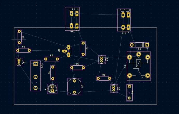
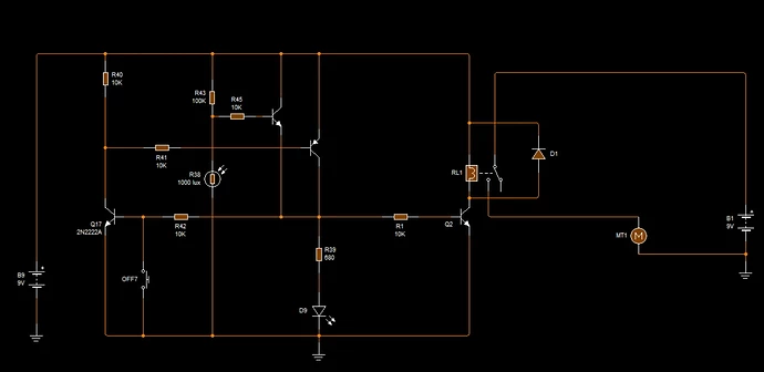
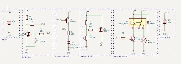
Hello there I'm having a problem designing my first PCB on Kicad my problem is with footprints placement or how to place footprints the best way possible for easy routing.
it's driving me crazy I've tried a lot to place the footprints the best way possible but the end up like a mesh of wires.
what advice can you give me to best place these components
I'm designing this PCB as a single-layer circuit
Excuse my horrible English.
All the best on your first PCB!
Placement of the components are always about trial&error and following certain guidelines. Here’s a video on how to select the components and arrange them on a PCB : link (from 7:00)
My suggestions would be :
- First place the components which are need to be interfaced with other devices or a person (like the display, buttons, ports, headpins, connectors, etc)
- Then place the major IC / large components / RF components (because this will have certain specification with routing or need more space than other passive components)
- Finally arrange the remaining and passive components around the main components, making sure to keep the shortest track distance the connections.
For more similar guidelines you can go through this
article.


