hello,
Subject Description : The PCB layout constraint for CSP package
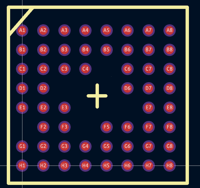
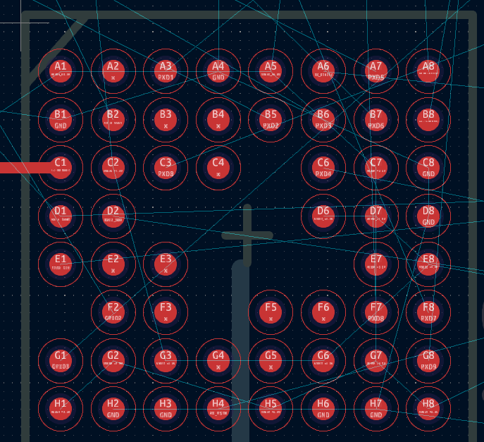
The CSP(like a BGA) package is shown as image_1.bmp. After schematics are translated into PCB editor, the component is shown as image_2.bmp. The red circle around a pad on image_2.bmp is automatically added by kicad, and the inner pad can not be connected with wire due to the red circle. my question is where i can change or modify it. The ball pith is only 0.55mm(V) and 0.6mm(H).
Thanks
Albert
The red circle is the clearance area. So, the tracks can’t go over it.
In latest version of KiCad there is no way we can set Global Clearance for the PAD, instead PAD clearance is derived from the net class of theconnecting wire.
So make sure that you set up the minimum track width under the design rules. Then set up a new net class with an appropriate track width that can travel between the pads. Finally assign the new netclass to the appropriate wires that we’ll connect those PADs.
You can learn more about it in this discussion here.

