pls check all routings and distance as per industry standard . Because we are going to make a prototype machine . otherwise pls tell me design constraint . so that i can chage .
Please share the PCB picture in the attachment next time, that should be sufficient to review it. You can drop your Gerber file here to convert your Gerber file into Pictures.
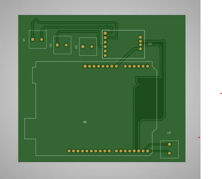
Check the attachment, I have marked the issues on the PCB.
- Red - Bad track
- Orange - not enough clearance
- Purple - Track too long
- Blue - Use the shortest path
PS : If you have further conversation on the same project/review, continue here (reply to this answer) don’t create a new question.
Thank you sir for your valuable review . I am sharing this file again with you . Pls check this file I have shred in the picture format.
The use of uno is just for showing after that we got some confident in PCB design understanding we remove all unwanted things.
Sir currently I’m facing problem with like off grid pin . Pls tell me how to do . thank you sir
Not perfect, but this look better than before. Just increase the copper pour clearance and it should be good to go for your first PCB.
off grid warning is already answered in thisquestion
This topic was automatically closed 24 hours after the last reply. New replies are no longer allowed.