Hi,
I am pcb file form altium. I am working on a printed PCB antenna that has traces at the bottom on an FR-4 substrate. Unfortunately, the dimensions or any other details of the design of the circuit have not been provided by the authors of the paper which led to "guess work" on the footprint size and therefore non-uniformity in those traces. I need to fabricate this antenna. What possibly could be a solution in this case? I have no experience in Altium or Kicad which may take long to learn-redesign and do full wave simulations before fabrication.
paper: Parametric Optimization of a Non-Foster Circuit Embedded in an Electrically Small Antenna
for Wideband and Efficient Performance
If you just want to know the footprint size of a component that’s on the Image with no dimension, you can try this method. It’s not fool proof or accurate but it worked for me (You must have some known reference value on the image).
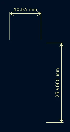
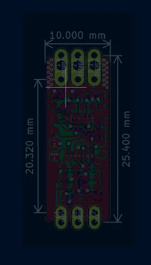
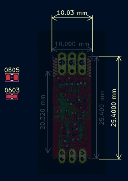
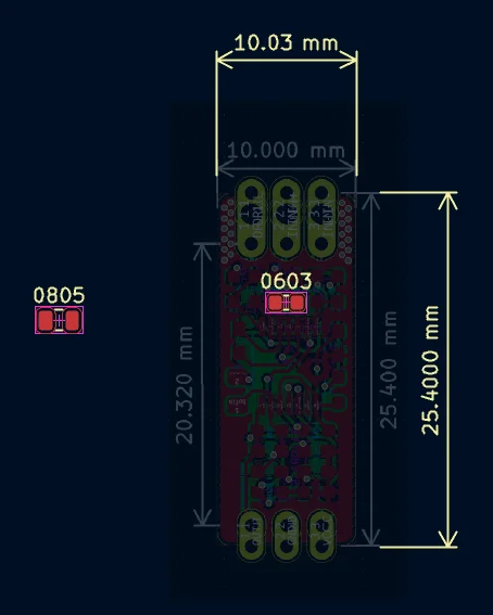
Step 1 - Add the known value on KiCad using “aligned linear dimension” tool
Step 2 - Import the Image on KiCad using the “Add bitmap Image” tool
Step 3 - Adjust the Image size until it matches the known dimension
Step 4 - Then try placing the standard component of various size on the Image until you find something that’s similar to the footprint. This process can be followed to find the track width as well.
Once you know the Circuit, track width and footprint dimension, with little effort you can recreate the complete PCB.
Again this is not a fool proof or accurate way to find the footprint size, but it’s little better than “guess work” and can be done within KiCad. For more accuracy you can use the same method on a different CAD program (like Fusion 360).
Since the paper you shared is behind a paywall, I can’t say how this process of determining the track width will affect the PCB and the Antenna performance.
I am sharing the pdf here. What I am curious about is the fabricated pcb antenna seem to have a different footprint and trace width compared to the figures of the traces. Is there a way to do the same for the fabricated picture as well? I am using Kicad 6 so options are not very clear.
I don’t think we can do that in Fabricated PCB.
Usually Authors don’t make any money on the IEEE paper, so you can mail them your request and they should be happy to share the PCB layout.


